
")
Irradiation chambers for research, development and production
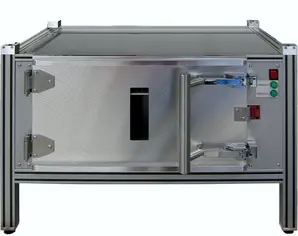
One core competence of Opsytec Dr. Groebel GmbH is development and manufacture of UV and daylight irradiation chambers. We offer irradiation chambers in different sizes and performance classes.
Highly efficient UV fluorescent lamps in the BS series produce much higher irradiance than the natural sun. The applications range from disinfection and UV aging to photostability testing.
With the compact UV LED chamber BSL-01i and the larger BSL-02, we offer you versatile irradiance chambers on a basis of high quality UV LEDs. The most common UV curing adhesives can be applied, due to the high irradiance of 100 mW/cm² to 200 mW/cm².
Compared to our standard BS series, the BSH-02 with UVC amalgam lamps offers irradiance that is 750% higher. So, the irradiance is high enough for high-energy applications or curing.
The BSM series uses medium-pressure Hg lamps for technical applications such as UV gluing and UV hardening. Due to the high irradiance and the built-in shutter, UV exposure is absolutely reproducible and completed within a few seconds.


")

BSH-03 CBD

BSH-03 UVC Collimated Beam Device: precise, collimated UVC irradiation for the disinfection and calibration of microorganisms in the laboratory. Learn more.
BSM-03 CBD
The BSM-03CBD is an irradiation chamber specially developed for the UV irradiation of liquid samples according to the colimated beam principle.
BS-OX
BS OX ozone-UVC irradiation chamber (185/254 nm) for surface activation, cleaning, and contact angle improvements
Applications of Irradiation Chambers
- Irradiation of bacterial and cell cultures
- Post-treatment for rapid prototyping / 3D printing
- Uniform irradiation of liquids in bags and blood plasma
- UV Curing of adhesives and polymers for small parts
- PCB and wafer irradiation
- Photostability of pharmaceuticals according to ICH Q1B
- Accelerated aging of plastics and similar materials with UV and daylight
- Surface disinfection
- Activation of polymer, glass, ceramic, and metal surfaces prior to bonding, sealing, or coating
- Cleaning of optical components, wafers, microchips, and filters with subsequent increase in the polar surface area
Adjustment of contact angle
