

Market development of UV technology
UV technology is now part of numerous industrial, scientific and medical processes. Ultraviolet radiation is used to cure coatings, adhesives and photopolymers, to disinfect water, air and surfaces, in semiconductor manufacturing, for photochemical processes and in testing and measurement procedures.
At the same time, the underlying technology is changing. UV LEDs are opening up new applications through defined emission wavelengths, fast switching, compact designs and good integration capability. In parallel, increasing automation is raising the requirements for reproducible irradiation conditions, process monitoring and traceable UV measurement technology.
The available market studies use different definitions, reference years and system boundaries. Market volumes from different studies are therefore not directly comparable and cannot be added together. What is meaningful is above all the order of magnitude, the growth rate and the technological development within each field of application.
Market data as of September 2026.
UV technology as a growth market
The market development of UV technology is driven by several technological and economic factors. These include the increasing use of UV LEDs, the automation of industrial processes, higher requirements for quality assurance and traceability, and the growing use of optical methods in electronics, photonics, medical technology and environmental technology.
UV curing, UV-C disinfection and UV LED technologies are developing particularly dynamically. At the same time, UV processes are becoming more important within substantially larger markets such as semiconductor manufacturing, additive manufacturing, photonics and packaging technology.
Selected market indicators
| Field of application | Market indicator | Development |
|---|---|---|
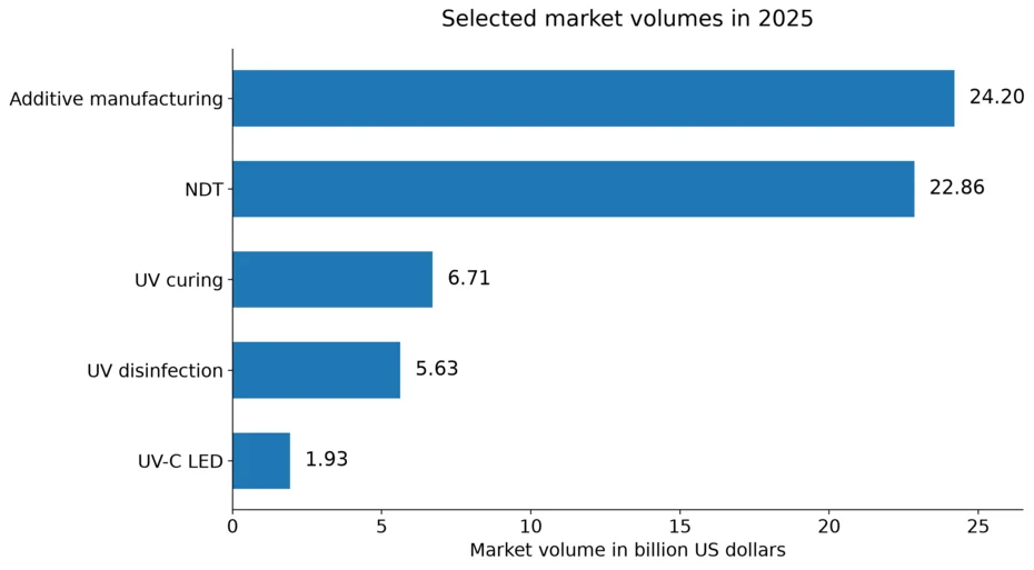
| Additive manufacturing | approx. USD 24.2 billion (2025) | +10.9 % compared with 2024 |
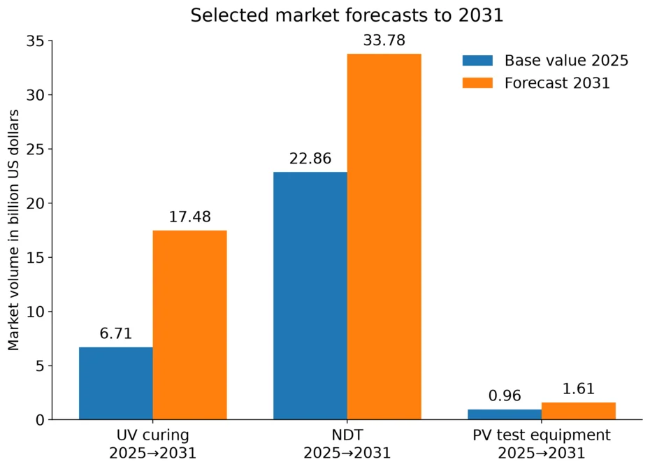
| UV curing systems | approx. USD 6.71 billion (2025) | approx. USD 17.48 billion by 2031 |
| UV disinfection equipment | approx. USD 5.63 billion (2025) | CAGR approx. 12.1 % to 2034 |
| UV-C LED | approx. USD 1.93 billion (2025) | CAGR just under 25 % to 2034 |
| NDT / non-destructive testing | approx. USD 22.86 billion (2025) | approx. USD 33.78 billion by 2031 |
| Photocatalysts | approx. USD 3.2–3.3 billion (2026) | CAGR approx. 8.7–8.9 % |
| Photovoltaic test equipment | approx. USD 0.96 billion (2025) | approx. USD 1.61 billion by 2031 |
The figures describe different markets with different market boundaries. They must not be added together to form an overall market for UV technology.
UV curing and UV LED technology
UV curing is one of the established industrial applications of ultraviolet radiation. UV radiation initiates photochemical reactions in coatings, printing inks, adhesives and other reactive materials. Short process times and immediate further processing make the method particularly attractive for automated production lines. Technology, standards and measurement tasks are described on the page UV Curing & Photopolymerization.
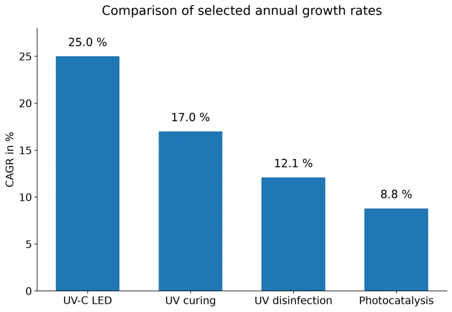
The global market for UV curing systems was estimated at around USD 6.71 billion for 2025. Growth to approximately USD 17.48 billion is forecast by 2031. This corresponds to an annual growth rate of around 17 % (Mordor Intelligence, 2026).
The radiation technology in use is changing in parallel. In 2025, mercury vapour lamps still accounted for a considerable share of the equipment market. UV LED systems are, however, growing at an above-average rate and are increasingly being integrated into new system concepts; the technical differences between the designs are summarised under UV LEDs for UVA, UVB and UVC.
For industrial UV curing processes, the electrical power of a radiation source alone is not decisive. What matters is the irradiance and the UV dose actually transferred to the material. Ageing, contamination, distance, temperature, production speed and optical components influence these quantities and therefore the process result.
UV-C and UV disinfection
UV-C radiation is used to inactivate microorganisms in water, air and on surfaces. The market for such systems is growing significantly, although the published market volumes vary considerably due to different definitions. Methods and measurement tasks are covered on the page UV Disinfection.
A global market volume of around USD 5.63 billion was reported for UV disinfection equipment in 2025. Under this market definition, an annual growth rate of about 12.1 % is expected through 2034 (Fortune Business Insights, 2025). Narrower or broader market segments arrive at values between about USD 1.5 and 6.4 billion for the same year (Global Market Insights; Mordor Intelligence).
The UV-C LED segment is developing particularly dynamically. A market volume of around USD 1.93 billion was reported for 2025; the forecast annual growth rate is just under 25 % through 2034 (Fortune Business Insights, 2025).
A key technological factor is the transition from mercury-containing discharge lamps to semiconductor-based radiation sources. Regulatory developments in the European Union and international measures to reduce mercury are reinforcing this change; the applicable deadlines are summarised under RoHS and UV lamps.
As UV-C systems become more widely used, the metrological determination of the effective irradiance and fluence is gaining importance. This applies in particular to validated disinfection processes, in which the applied UV dose must be traceable and reproducible.
Additive manufacturing and photopolymerisation
UV-based polymerisation is a central process in various additive manufacturing methods. In stereolithography and related methods, light-sensitive resins are exposed and cured locally. The page Additive Manufacturing & 3D Printing describes the individual process steps.
According to the Wohlers Report 2026, global revenue in the additive manufacturing industry reached around USD 24.2 billion in 2025. This corresponded to growth of 10.9 % compared with the previous year. Other market analyses arrive at higher figures due to broader definitions and continue to forecast double-digit growth rates (Grand View Research, 2025).
With increasing industrial use, the requirement is shifting from mere part production to reproducible series manufacturing. The optical power, spectral distribution and homogeneity of the exposure influence polymerisation, part geometry and material properties. Controlled UV exposure thus becomes part of process quality.
UV processes in the automotive industry
In vehicle manufacturing, UV radiation is used to cure adhesives, coatings and potting compounds, among others in headlights, displays, sensors and trim components. Applications and test requirements are described on the page Automotive & Vehicle Components.
There is no separate market size for “UV curing in the automotive industry”, as UV-curing systems are delimited differently from study to study. The market for UV-curable adhesives serves as an adjacent indicator: a global volume of around USD 5.15 to 5.43 billion is reported for 2025/2026, with an expected annual growth rate of about 5.5 % through 2031 (Mordor Intelligence, 2026); a different delimitation puts the market at around USD 4.53 billion for 2024 with growth of about 5.2 % (TechSci Research, 2024).
For manufacturing, the cycle time matters more than the absolute market size: with short exposure times and tight distance tolerances, the UV dose actually achieved determines whether a bond reaches the required strength.
Packaging and filling technology
In filling technology, UV-C radiation is used to disinfect packaging materials, closures, conveyor belts and product surfaces. The page Packaging & Filling Technology describes the associated measurement tasks.
No separate market for UV germ reduction in packaging is reported. Packaging machinery serves as an indicator: the VDMA reported production by German food and packaging machinery manufacturers of just under EUR 17 billion for 2025, of which around EUR 9 billion is attributable to packaging machinery, with an industry export share of about 80 %. As an adjacent indicator, aseptic packaging is estimated at around USD 77 to 89 billion for 2025, with annual growth rates between 8 and 11 %.
The high export share is technically significant: equipment must be verifiable in different regulatory environments, and for UV processes verifiability requires a measurable fluence.
Electronics and semiconductor manufacturing
In the electronics and semiconductor industry, UV radiation is used for photolithography, cleaning, surface activation and photochemical process steps, among other things; the individual process steps are covered on the page Electronics & Semiconductor Industry.
There is no separate market statistic for UV processes within semiconductor manufacturing. The development of adjacent capital equipment markets does, however, indicate the economic order of magnitude of the manufacturing processes concerned. A global volume of around USD 165.9 billion was forecast for semiconductor manufacturing equipment in 2026. Of this, around USD 143.9 billion is attributable to wafer fab equipment (SEMI, Mid-Year Forecast 2026).
Particularly high requirements arise wherever small process deviations have a large effect on yield and component quality. The characterisation of optical radiation sources and the monitoring of UV processes are therefore part of an increasingly precise and automated manufacturing environment.
Optics, photonics and precision components
Photonics is a significant industrial technology market. For Germany, industry revenue of around EUR 50 billion with an export share of 76.3 % was reported for 2024 (SPECTARIS, key figures 2025). Worldwide, photonic components and materials cover markets in the hundreds of billions (Photonics21/TEMATYS, Market Research Study Photonics 2024).
In optics manufacturing, UV technologies are used for cleaning, surface activation, bonding, coating and testing, for example. As the requirements for optical systems increase, so do the requirements for process stability and quality assurance; the page Optics & Precision Components examines the individual process steps.
In high-quality optical assemblies, even a small deviation within a single process step can affect the function of the entire system. Metrological monitoring of UV irradiation therefore represents a comparatively small effort within the value chain, yet it can contribute substantially to reproducibility.
Lighting technology, LED and display technology
In lighting and display technology, UV processes are used for curing, encapsulation and surface treatment; at the same time, the spectral characterisation of the light sources themselves is a measurement task. The page Lighting Technology, LED & Display Technology covers both aspects.
The market for LED displays was reported at around USD 19.7 billion for 2025, with an expected annual growth rate of about 5.4 % through 2031 (Mordor Intelligence, 2025). For the LED lighting market, estimates for 2025 range between around USD 100 and 110 billion, with growth rates of 8 to 13 % depending on the delimitation (Grand View Research, 2025; Fortune Business Insights, 2026).
Water and environmental technology
Water and wastewater treatment are among the most important fields of application for UV disinfection. UV methods enable the physical inactivation of microorganisms without the direct addition of chemical disinfectants; the page Water & Environmental Technology compares the methods.
Market analyses continue to expect double-digit growth rates for UV disinfection technology. At the same time, the market for UV LEDs is growing considerably faster. This development broadens the design options for compact UV systems that can be switched on demand and controlled electronically.
For the technical assessment of such systems, the optical power alone is not sufficient. What is decisive is the fluence that actually reaches the medium to be treated. Sensors and radiometry therefore form an important basis for validation, monitoring and maintenance – the procedure is described on the page UV reactor validation.
Further growth markets for UV technology
UV technologies are part of numerous other markets, even where no separate market size is reported for the UV share.
Photocatalysis
Photocatalytic processes use light to activate suitable materials, in particular titanium dioxide. The market for photocatalysts is estimated at around USD 3.2 to 3.3 billion for 2026. Annual growth rates of about 8.7 to 8.9 % are expected (Mordor Intelligence, 2026; Persistence Market Research, 2026). More on this on the page Photocatalysis.
Photovoltaics and solar simulation
Solar simulators and optical test methods are used in research, development and quality assurance of photovoltaic cells and modules, see Photovoltaics & Solar Simulation. As an adjacent market indicator, the market for photovoltaic test equipment was estimated at around USD 0.96 billion in 2025; growth to approximately USD 1.61 billion is forecast by 2031, corresponding to around 8.75 % per year (Mordor Intelligence, 2026).
Laser processes and transmission testing
In laser transmission welding of plastics, the transmission of the upper joining partner determines the energy introduced; testing this transmission is part of material release, see Laser Processes & Transmission Testing. There is no separate market definition for transmission testing itself. The market for laser plastic welding serves as an indicator and is put at around USD 1.5 to 1.7 billion for 2025; about USD 2.3 to 2.7 billion is expected by 2032, corresponding to 5 to 8 % per year.
Pharmaceutical photostability testing
Photostability tests examine the effects of optical radiation on medicinal products and active substances. They are part of stability testing defined by regulation under ICH Q1B, see Pharma & Photostability. The overarching market for pharmaceutical stability and storage services was estimated at around USD 1.92 billion for 2024 (Grand View Research, 2025).
Photobiology and medical phototherapy
UV-A and UV-B radiation are used in photobiological research and medical phototherapy, see Photobiology & Biotechnology and Medicine & Phototherapy. Market definitions differ considerably here, as devices, treatments and individual indications are delimited in different ways. For measurement technology, spectral weighting, irradiance and dose are particularly relevant.
Plant cultivation, agriculture and food technology
UV radiation is used in controlled plant cultivation systems, to influence biological processes and for hygiene applications, see Plants, Agriculture & Food Technology. The associated markets – including vertical farming, horticultural lighting and UV germ reduction – show high growth rates in some cases. The actual UV share cannot, however, be delimited as a separate overall market.
Non-destructive testing
In fluorescent penetrant testing, UV-A radiation excites fluorescent test media, see Fluorescent Penetrant Testing & Industrial Inspection. The global market for non-destructive testing was estimated at around USD 22.86 billion for 2025 and is expected to grow to approximately USD 33.78 billion by 2031 (Mordor Intelligence, 2026).
In safety-critical industries such as aerospace, defined UV-A irradiation is part of standardised test conditions. Controlling irradiance and ambient light is therefore directly linked to the quality of the test procedure.
Photobiological safety in the workplace
No separate global market is recorded for photobiological safety in the workplace; the requirements follow from standards such as IEC 62471 and EU Directive 2006/25/EC, see Occupational Safety & Photobiological Safety. The LED lighting market serves as an indicator: it is put at around USD 97 to 109 billion for 2025 and grows at 8 to 14 % per year depending on the delimitation (Fortune Business Insights, 2026).
What is technically relevant is not the market size but the shift in spectral distribution: compared with incandescent and halogen lamps, LEDs emit a higher blue content at the same illuminance, which makes blue light hazard according to IEC 62471 a separate test criterion for general lighting as well.
From the UV lamp to the controlled UV process
The economic development of UV technology cannot be described by growing market volumes alone. Of greater technical significance is the transition from the radiation source to the controlled UV process.
In industrial applications, it is not decisive merely whether UV radiation is present. Relevant factors include:
- spectral irradiance,
- UV dose or fluence,
- spatial homogeneity,
- stability over time,
- distance and geometry,
- temperature dependence,
- ageing of the radiation source,
- contamination of optical components,
- production speed and exposure time.
These influencing variables determine which optical radiation actually reaches the workpiece, medium or biological target.
With increasing automation and rising quality requirements, the importance of UV sensors, radiometers, dosimeters and spectral measurement technology is therefore growing. Traceable calibrations from the accredited calibration laboratory make it possible to compare measured values across development, production, quality assurance and service. Which sensor suits a given task can be narrowed down with the UV Sensor Finder.
The development of UV technology is thus at the same time a development towards measurable, verifiable and automatable UV processes.
Putting the market forecasts in context
Market studies are not a uniform statistical database. Providers use different definitions for products, regions, value-chain stages and forecast periods.
A market for “UV disinfection”, for example, may comprise complete devices only, or additionally take into account UV lamps, LED modules, sensors, services and system components. Similar delimitation problems exist for UV curing, photonics, photocatalysis and medical applications.
Three consequences follow from this:
- Market volumes from different studies cannot be added together.
- Diverging market figures need not be contradictory if different system boundaries are used.
- Growth rates and technological trends are often more meaningful than a single absolute market size.
Taken together, the available data nevertheless shows a consistent technological development: UV technologies are being used in a growing number of industrial and scientific processes. UV LEDs, automated manufacturing, validated disinfection processes and rising quality assurance requirements are at the same time increasing the need for precise optical measurement technology.
Sources and further market studies
The market figures are based on published sources and market studies. These include, among others:
- ASTM International – Wohlers Report 2026 (additive manufacturing)
- SEMI – Mid-Year Forecast 2026 (semiconductor manufacturing equipment and wafer fab equipment)
- WSTS – Spring Forecast 2026 (semiconductor market)
- SPECTARIS – key figures 2025 (photonics in Germany)
- Photonics21 / TEMATYS – Market Research Study Photonics 2024
- Mordor Intelligence – UV Curing, UV Disinfection, Non-Destructive Testing, Photocatalyst, UV Curable Adhesives and LED Display
- Fortune Business Insights – UV Disinfection Equipment, UV-C LED and LED Lighting
- Grand View Research – Additive Manufacturing, Photopolymers, Pharmaceutical Stability & Storage Services and LED Lighting
- Global Market Insights – UV Disinfection Systems
- Persistence Market Research – Photocatalysts
- TechSci Research – UV Curable Adhesives
- Yole Group – advanced packaging and photonic applications
- VDMA – food and packaging machinery 2025
- Future Market Insights – Photostability Chamber
Note: Market data changes continuously. The figures serve to place technological fields of application in economic context and do not constitute a market forecast by Opsytec.
Author: Dr. Mark Paravia
Dr.-Ing. Mark Paravia is the managing director of Opsytec Dr. Gröbel GmbH in Ettlingen and heads the accredited calibration laboratory. Following his research on pulsed xenon excimer discharges at the Institute of Lighting Technology at KIT, his focus today is optical radiation measurement. He is vice-chair of the DIN standards committee FNL 7 “Optical radiation” and a member of the DVGW project group on UV disinfection.