


Designing UV bonding, potting and encapsulation reliably
In UV bonding, potting and encapsulation it is the radiation in the reaction zone that decides the process – not the nominal rating of the source. Parts act as optical filters; bond gap, layer thickness, pigments and shadowed areas change the radiation that actually arrives. A sound design therefore ties material data, part transmission, irradiation geometry, dose and temperature to a defined acceptance criterion at the workpiece.
Which material comes into question at all is covered under selecting UV-curing adhesives, coatings and potting compounds; the reaction mechanism and the process variables of curing are explained in the fundamentals of UV curing and photopolymerization. This page starts where the material is settled and the process has to be laid out on the real part.
Six typical processes and their critical quantity
UV bonding, potting and encapsulation are used wherever a joint needs to cure quickly, precisely and without thermally stressing the component. A different quantity is decisive in each process:
- Optical bonding (lenses, prisms, camera modules): The adhesive sits behind glass or a coating – and that coating may block exactly the band the photoinitiator needs. Part transmission and shrinkage are critical, because shrinkage pulls the alignment out.
- Displays and touchscreens: A large, thin gap on a tight cycle time: here it is the uniformity of irradiance across the area that decides, not the peak value in the centre.
- Sensor and connector potting: Potting heights of one to several millimetres and housing walls that cast shadows. The critical question is whether the minimum dose still arrives at the bottom of the potting – or whether a dual-cure system is needed.
- Printed circuit boards and densely populated assemblies: Tall components cast shadows on neighbouring bond sites. Irradiation geometry and angle of incidence are critical, not the power of the emitter.
- Battery modules and power electronics: Large, partly curved joining surfaces with a limited temperature budget. Releasing dose and part temperature together is the critical step.
- Medical technology and microfluidics: Small gaps, tight tolerances and releases that must be documented. A reproducible measuring location that actually represents the joint position is critical.
What matters about the adhesive for process design
UV- and light-curing adhesives consist of monomers or oligomers and a photoinitiator that decomposes into reactive species at the matching wavelength and starts cross-linking. Reaction pathways, oxygen inhibition and the governing process variables are derived in the fundamentals of UV curing and photopolymerization.
For designing a bonding or potting process, three figures from the data sheet matter: the absorption range of the photoinitiator, the minimum dose, and whether the system has a second curing path independent of radiation. Everything else is decided at the part.
What Distinguishes a Bondline from a Coating?
A coating is exposed to ambient air; there, oxygen at the surface is the main issue. A bondline, by contrast, is usually covered – it is irradiated through the component or from the side, with correspondingly less oxygen ingress. What matters more here is the spectral transmission of the component and the geometry of the joint. The underlying relationships between spectrum, dose rate and crosslinking are summarised under UV Curing & Photopolymerization.
Wavelength: what has to be settled at the part
A photoinitiator absorbs only within a limited band – a more powerful source at the wrong wavelength will not excite it. Which properties distinguish the industrial LED peaks at 365, 385, 395 and 405 nm, and which photoinitiator systems match them, is compared on the technology page on UV LEDs for UVA, UVB and UVC [1].
For process design, all that counts is what still arrives behind the real part – and that is exactly what the following rule decides.
A decision rule instead of the nominal LED wavelength
The wavelength is derived from the absorption range of the photoinitiator and the transmission of the complete part assembly. Shorter wavelengths can be strongly absorbed at surfaces, while longer UVA or violet wavelengths often penetrate transparent substrates and greater layer thicknesses better.
What governs the choice is therefore a spectral measurement behind the real part, or on a representative process geometry; a blanket assignment by nominal LED wavelength is not sufficient. The properties of the individual peaks – full width at half maximum, manufacturing tolerance and the shift with junction temperature – are compared on the technology page on UV LEDs for UVA, UVB and UVC.

How Does the Joining Part Act as an Optical Filter?
The transmission of the component decides which part of the spectrum even reaches the adhesive. Optically clear does not mean UV-transparent: many plastics that look water-clear in the visible range fall off steeply below roughly 380 nm; float glass is nearly opaque in the UVB range; and UV-blocking additives in housing materials exist for exactly that purpose. In practice, this means the transmission curve of the joining part and the absorption band of the initiator must overlap. Where that overlap is narrow, the options shift towards a longer wavelength, irradiating from the joint side, dual-cure systems that offer a second curing path via heat or moisture, and light-activated adhesives that keep reacting after exposure.
Spot or Area – What Role Does Geometry Play?
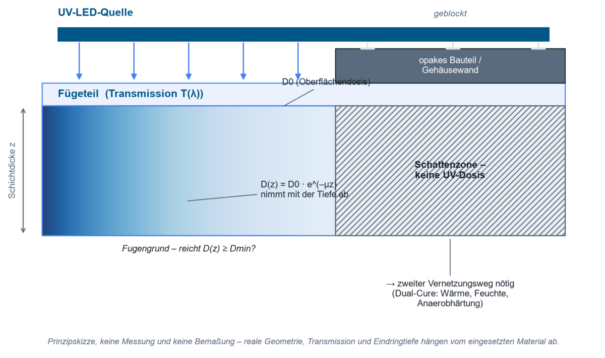
Small dots of adhesive (connectors, sensors, populated PCBs) suit a UV-LED spot source with high irradiance over a few mm². Longer seams or several parts cured at once suit area sources or modular line-array systems along a conveyor. The real design question is not spot versus area, but shadowing: housing edges, metal frames, opaque components and undercuts create zones that cannot be reached. It pays to calculate the irradiance field before building the equipment via optical simulation, which works on imported component geometries. An unreachable zone is not a design detail to be tolerated – it calls for a second curing mechanism, covered in the section on dual-cure systems.
UV Adhesives for Electronics, Sensors, Optics and E-Mobility
In electronics and semiconductor manufacturing, UV adhesives are increasingly taking on tasks that were traditionally reserved for soldering: component bonding, conformal coating and display assembly can be achieved at lower process temperatures and shorter cycle times than soldering or thermally curing systems. In sensors, tight fit tolerance for small components matters most; in optics, it is dimensional stability – which is why cationically curing epoxy systems are more often used instead of acrylates there, thanks to lower shrinkage, particularly for bonding glass, metal and polymer in optical assemblies.
E-mobility brings its own constraints: rising power density alongside shrinking installation space, higher requirements for temperature, chemical and mechanical resistance, and increasingly flexible substrates and flex-PCBs on curved surfaces. For battery modules, power electronics and sensors in drivetrains, this means UV adhesives must not only fixture quickly but remain stable over the vehicle's service life.
UV Potting and Encapsulation: Layer Thickness and Shadow Areas
Potting compounds and encapsulants have a layer thickness that a bondline does not. Radiation is absorbed and scattered over depth – the surface reacts first and the bottom zone last, and with filled, pigmented or turbid compounds, sometimes not at all. Penetration depth depends simultaneously on filler, colour, photoinitiator concentration and layer height, and cannot be derived from surface irradiance alone. In electronic assemblies, the thermal side adds to this: a UV-LED carries almost no infrared load, but part of its optical power still converts to heat in the material, and crosslinking itself is exothermic. For temperature-sensitive components, component temperature must therefore be tracked alongside dose – shorter exposure at higher power is not automatically the gentler option.
Why Does UV Intensity Decrease with Layer Thickness?
The cause of this attenuation is absorption by the matrix material and the photoinitiator: every additional increment of thickness consumes a constant fraction of the remaining radiation. For clear, homogeneously absorbing systems, this can be approximated with the Beer-Lambert law:
I(z) = I₀ · e−αz
where I₀ = incident irradiance, I(z) = irradiance at depth z, α = effective absorption coefficient.
At constant exposure time, the cumulative dose D(z) follows the same exponential form – the worked example below uses the more common coefficient µ instead of α, physically the same quantity.
For filled potting compounds, this simple model is often not enough, because scattering at pigments, fillers and interfaces adds to the picture – the radiation is not only absorbed but also weakened further along a longer, diffuse path.
Worked Example: Does the Surface Dose Reach the Bottom of the Joint?
Attenuation of the radiation over layer thickness can be estimated in simplified form with the Lambert-Beer law:
D(z) = D₀ · e−µz
where D₀ = surface dose, D(z) = dose at depth z, µ = material-dependent extinction coefficient.
Illustrative assumptions for a 2 mm thick, lightly filled epoxy potting compound at 365 nm:
- Required minimum dose at the bottom of the joint (per adhesive datasheet): Dmin = 1,500 mJ/cm²
- Measured residual transmission of the compound at 2 mm layer thickness: T ≈ 30 % (values for similar filled systems typically fall in the 20–40 % range depending on filler content and should be measured on the real material)
This gives the required surface dose:
D₀ = Dmin / T = 1,500 mJ/cm² / 0.30 ≈ 5,000 mJ/cm²
If the equipment, within the allowed process window (time, temperature budget), delivers only, say, 3,000 mJ/cm² at the surface, the bottom of the joint is left at roughly 900 mJ/cm² – below the minimum dose. The batch cures through at the surface but not at the bottom. Options in that case: reduce layer thickness, switch to an adhesive with higher transmission at the chosen wavelength, add irradiation from the side, or move to a dual-cure system. The actual transmission of a potting material can be measured on a material sample with a spectroradiometer, rather than estimated from datasheet values.
The transmission of the joining partner decides how much of the surface dose reaches the bond line. A measured transmission gives the optical density and vice versa; with several layers in the beam path their transmissions multiply. In detail in the transmission and optical density calculator.
The calculator runs entirely in your browser — no data is transmitted.
Dual-Cure Systems for Areas That Cannot Be Irradiated
UV radiation travels in straight lines and cannot bend around obstacles. Tall components on a PCB (electrolytic capacitors, connectors, coils), undercuts, cavities, or a closed housing irradiated from outside all create shadow areas where the adhesive stays liquid without an additional measure. Dual-cure adhesives solve this via a second, UV-independent curing path:
| Dual-cure type | Secondary mechanism | Typical use |
|---|---|---|
| UV + heat | Temperature held for a defined time (e.g. 15–30 minutes at 125–150 °C) | Maximum strength and temperature resistance; raises the glass transition temperature on top of the UV cure |
| UV + moisture | Ambient humidity over a set time (e.g. 24 hours) | Large gaps or assemblies where post-curing with heat is not practical |
| UV + anaerobic cure | Curing in the absence of oxygen, in the presence of metal ions | Potting or bonding deep inside metal assemblies, e.g. thread locking |
Practical tip for detection: a UV indicator film at the bond site, exposed under production conditions, makes shadow areas visible as unexposed spots before the first production run.
Designing and releasing the process: six steps
The design follows a fixed order; each step presupposes the one before it:
- Document the material system and the permissible process window.
- Check the transmission of substrate, coating and bond gap in the relevant spectral range.
- Choose source and geometry so that edge and shadowed zones are reached as well.
- Capture irradiance and dose at a representative measuring location.
- Qualify temperature and cycle time together with the curing result.
- Define limits for series monitoring, alarm and recalibration.
A cured bond cannot be checked visually. Because the decisive process variable is invisible, every approved bonding process needs a measured value: the irradiance at the joint position and the resulting dose. For initial process design and comparing sources, the UVpad delivers the spectrum at component level; for recurring checks, a broadband radiometer such as the RMD Pro is sufficient. Matching sensor and source matters: how far a broadband sensor can deviate against a narrowband LED spectrum is shown by the spectral mismatch.
Alongside optical dose, temperature belongs in the same measurement chain: commercial UV radiometers do not capture infrared irradiance, so the thermal effect is usually captured as a rise in component temperature via a non-contact pyrometer [2]. Heat can be a benefit or a risk depending on the application, but it is always part of the process window – for temperature-sensitive components (electronics, optical cements) it should be released and monitored just as rigorously as the dose itself.
Which instruments capture irradiance and dose at the measuring location is shown by the product overview of measuring UV dose and irradiance.
Process Monitoring in Industrial UV Bonding
In series production, measurement moves into the line: UV curing sensors stay permanently in the beam path, and curelog records up to 2,000 measurements per second across four spectral ranges, making the profile of a fast-running curing line visible. Both approaches answer the same question – is the source still operating within its approved window? That it does not stay there automatically over time is described under ageing of UV lamps and UV-LEDs: peak wavelength and output power shift, often slowly enough to go unnoticed during ongoing operation until parts fall outside the approved window. More broadly, this trend towards continuous inline monitoring is also visible among other manufacturers of UV curing systems in the context of Industry 4.0.
For trial series and material approvals away from the line, irradiation chambers with defined geometry are available, plus, for the process side, control units with timer, dimming and trigger functions, and the rest of the UV-LED light source range.
What Do Scientific Publications Show?
Our own customer publications also show UV bonding in several facets – from surface pretreatment for bonded joints to encapsulation of photovoltaic modules.
Examines how a UVO pretreatment changes the interlaminar toughness of co-extruded epoxy-LMPAEK bonded joints – evidence that UV treatment does not just cure, but can affect joint strength itself.
Hybrid epoxy-LMPAEK composite co-cured joints: A study on UVO pretreatment and its effect on interlaminar toughness
Katz, L., et al. "Hybrid epoxy-LMPAEK composite co-cured joints: A study on UVO pretreatment and its effect on interlaminar toughness." Composites Part B: Engineering 323 (2026): 113727.
Monitors a silicone adhesive under UV exposure in high vacuum with a single multiparameter sensor – an application for the same kind of process monitoring that runs via a UVpad on the ground.
Multiparameter Single Sensor for Space Silicone Adhesive Monitoring Under High-Vacuum Ultraviolet Exposure
Fazzi, Luigi, et al. "Multiparameter Single Sensor for Space Silicone Adhesive Monitoring Under High-Vacuum Ultraviolet Exposure." Journal of Spacecraft and Rockets 60.3 (2023): 740-752.
Compares four encapsulant materials for photovoltaic modules under UV exposure in the Atacama Desert – encapsulation under extreme UV load, similar to what e-mobility assemblies can reach.
Comparing the effects of ultraviolet radiation on four different encapsulants for photovoltaic applications in the Atacama Desert
Correa-Puerta, Jonathan, et al. "Comparing the effects of ultraviolet radiation on four different encapsulants for photovoltaic applications in the Atacama Desert." Solar Energy 228 (2021): 625-635.
Examines the oxygen-affected layer in multilayered photopolymers – the effect that leaves the surface tacky while the core is already fully crosslinked.
Effect of the oxygen affected layer in multilayered photopolymers
Pierrel, J., et al. "Effect of the oxygen affected layer in multilayered photopolymers." Polymer Chemistry 8.31 (2017): 4596-4602.
Shows, for ultrafast-curing acrylates, how comonomer choice and amount shift the thermomechanical properties of the crosslinked network.
Influence of co-monomer-type and amount on thermomechanical properties of ultrafast-curing acrylic resins using a triacrylic crosslinker
Böhm, Michael, et al. "Influence of co-monomer-type and amount on thermomechanical properties of ultrafast-curing acrylic resins using a triacrylic crosslinker." Journal of Applied Polymer Science 136.13 (2019): 47294.
Further work from the photochemistry and polymer research, and stereolithography, crosslinking and coatings topic fields is listed under Publications by customers – by topic.
The publication finder lists all publications on bonding and potting we know of – searchable by device, field and keyword.
Technical Background and Further Reading
[1] : ScienceDirect – Specific photoinitiating systems at 365, 385, 395 and 405 nm
[2] : uvmeasurement.org – Radiometric Methods for UV Process Design and Process Monitoring
FAQ on designing UV bonding and potting processes
Which wavelength suits my UV adhesive?
What governs this is the overlap between the source spectrum and the absorption band of the photoinitiator, together with the transmission of the joining part. The adhesive data sheet is binding, confirmed by a spectral measurement behind the real part – the nominal LED designation alone is not sufficient.
How deeply does UV radiation penetrate a potting compound?
Penetration depth approximately follows the Lambert-Beer law and depends on filler, colour, photoinitiator concentration and wavelength. It cannot be derived from surface irradiance alone; it has to be measured on the real material, for example with a spectroradiometer.
What are dual-cure adhesives and when are they needed?
Dual-cure adhesives combine fast UV fixturing with a second curing path independent of UV (heat, moisture or anaerobic). They are used when shadowed zones – under tall components or inside closed housings, for instance – cannot be irradiated sufficiently.
Where is the UV dose measured in bonding?
At the joint position, not at the emitter housing and not on top of the part when the adhesive lies underneath. The measuring location has to represent the least favourable point of the real assembly; the spectral match between sensor and source matters in addition, because a poorly matched broadband sensor returns markedly deviating readings under narrowband LEDs.
Which acceptance criterion releases a UV bonding process?
A cured bond cannot be inspected visually. Release is therefore given against a pair of values – minimum dose at the measuring location and permissible part temperature – backed by the curing result from qualification, plus limits for alarm and recalibration in series production.
How can a UV bonding process be monitored in series production?
Through UV curing sensors permanently installed in the beam path and continuously logging instruments that compare irradiance and dose against the released process window at all times and report deviations – from ageing of the source, for example – in real time.
Which UV adhesives suit electronics manufacturing and e-mobility?
Depending on the requirement, free-radical curing acrylates (fast fixturing) or cationically curing epoxies (low shrinkage, high temperature and chemical resistance), often as a dual-cure system for shadowed zones on densely populated assemblies.
Related application fields
Bonding with light borders directly on three further fields: UV curing and photopolymerization provides the fundamentals on initiator, spectrum and oxygen inhibition, electronics and semiconductor manufacturing uses the same potting and encapsulation steps in the back end, and in the automotive industry battery modules and power electronics keep creating new, often heavily shadowed bond geometries. Added to these are automation and process integration for in-cycle monitoring and optics and precision components for joining optical parts. Where the adhesive is dispensed by a robot and cured directly at the point of application, path geometry is added as an influencing factor – see robotics. The full picture is in the UV applications overview.
Author: Dr. Mark Paravia
Dr.-Ing. Mark Paravia is the managing director of Opsytec Dr. Gröbel GmbH in Ettlingen and heads the accredited calibration laboratory. Following his research on pulsed xenon excimer discharges at the Institute of Lighting Technology at KIT, his current focus is on optical radiation measurement technology. He is vice-chair of the DIN Standards Committee FNL 7 “Optical Radiation,” and a member of the DVGW Project Group on UV Disinfection.
Get Advice on Your UV Bonding Process
Not sure whether your UV dose still reaches the bottom of the joint? We measure your spectrum and irradiance on the real component and advise you on the right wavelength, geometry and process monitoring – send us your question or request a UVpad measurement directly.